We have several threads on red-gray chips to choose from for what I am going to post now. I chose this, because it's where Sunstealer first published his finding that the MEK-soaked chip is probably Tnemec (post 536).
On my blog, Ivan Kminek reported an observation about the data on that MEK-soaked chip that I find interesting and worthwhile pursuing:
http://oystein-debate.blogspot.de/2...howComment=1337005281901#c1942663736651428010
The problem he's discussing is the apparent observation that some unspecified region of that chip, after soaking, contains mostly Al, and too little O to have all the Al oxidized:
[qimg]http://i1088.photobucket.com/albums/i328/MikeAlfaromeo/ActiveThermiticMaterial/ActiveThermiticMaterial_Fig17.jpg[/qimg]
This finding has always had me wondering, and I admit I didn't have an explanation, and considered that measurement to be somehow erroneous, perhaps even faked. But having any fake data in the paper was not an option I could have been happy with at all.
Now Ivan asks a good question:
Could it be a question of probe geometry that made the Al-count so much greater than the O-count in that XEDS measurement?
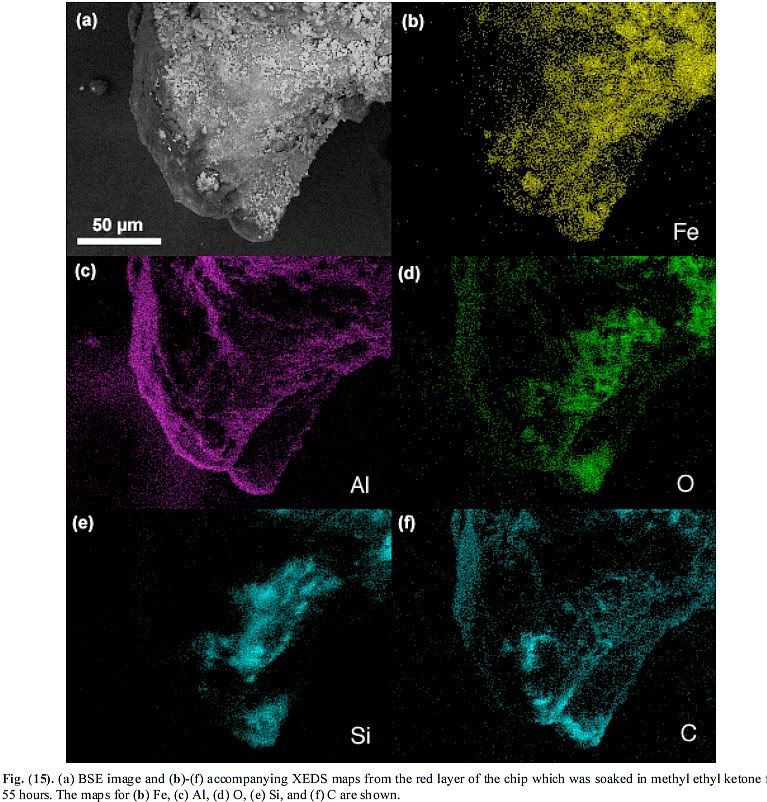
I can't give a direct, or experimental, answer to this, but there is a good indication that something of that sort is at play here, namely the distribution of oxygen as per the XEDS map, Figure 15:
[qimg]http://i1088.photobucket.com/albums/i328/MikeAlfaromeo/ActiveThermiticMaterial/ActiveThermiticMaterial_Fig15.jpg[/qimg]
You will notice that the heavy iron appears pretty ubiquitiously, but C and O do not. O supposedly is associated with Fe as iron oxide, and it is the most common element in that chip as per Fig.14, so it is a bit curious that it would not show more and more ubiquitiously. It seems like for some reason, the K-alpha level of O gets attenuated somehow in that experiment.
Another observation: While there are some scattered dots for all 5 elements outside of the confines of the chip itself, the signal for Al outside of the chips looks pretty significant. Could this come from the crucible of the XEDS device? And the concentrated Al signal on the "southwestern" edge of the chip a reflection from the Al-crucible?
I find it quite conceivabe that the geometry edges of the chip, which are far from being perpendicular to the "line of sight", precludes much of a signal from the probe to reach the detector, and that the strong Al-signal comes not from the probe, but from the crucible!
Any comments from those who know SEM equipment?
 )
)
")


")